行业
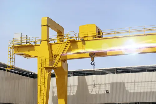
VAHLE Crane Technology
Individual solutions for heavy loads

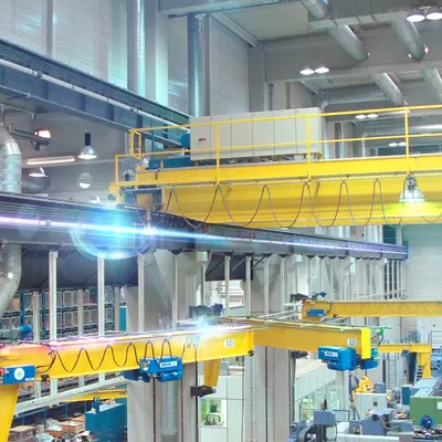
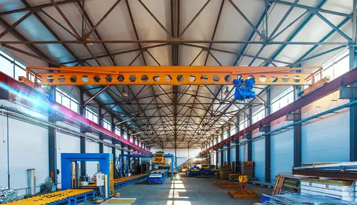
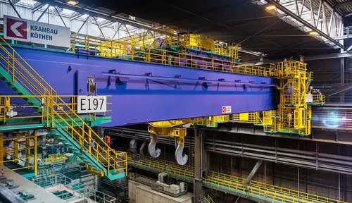
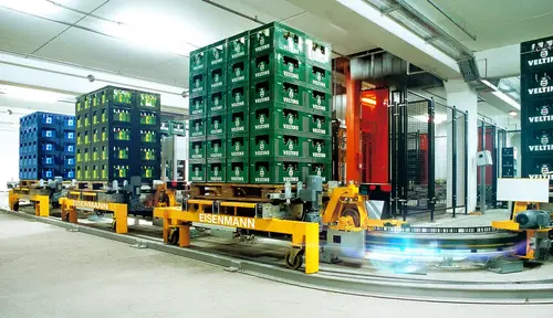
Cranes are used in many industries. Steel producers, recycling yards and companies from the construction industry VAHLE offers reliable systems for energy and data transmission.

Discover solutions
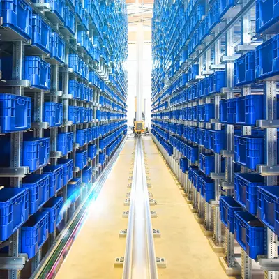
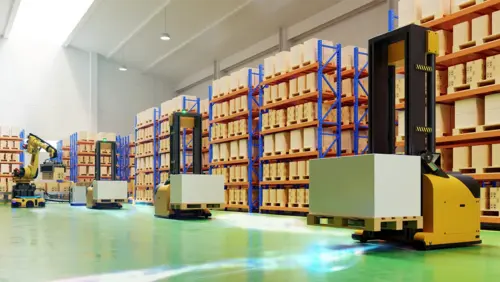
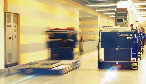
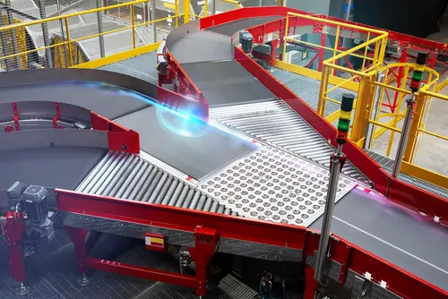
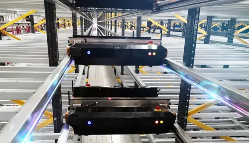
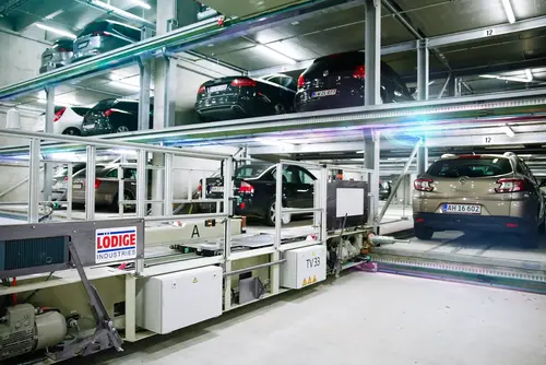
VAHLE Intralogistics automated small parts warehouse
Automated conveyor technology in the internal flow of goods

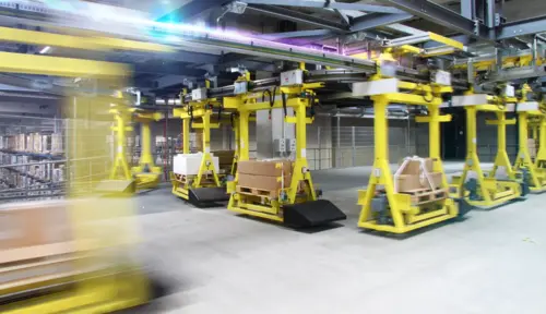
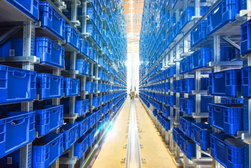
Increasing production rates, high throughput volumes and short delivery times require partially or fully automated intralogistics.

Discover solutions
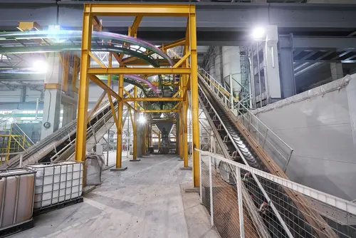
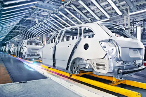
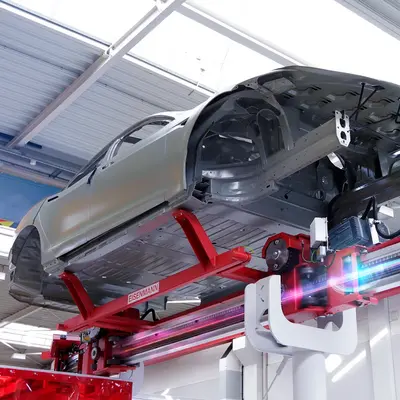
VAHLE Automotive Electric Monorail System (EMS)
Innovative solutions for flexible production processes

Adaptable manufacturing processes are the key to the greatest possible efficiency in vehicle production. VAHLE solutions for energy and data transmission make a significant contribution to this.

Discover solutions
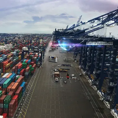
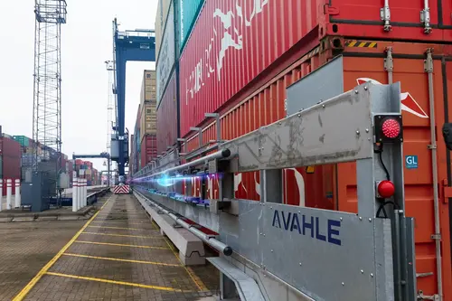
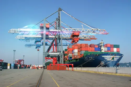
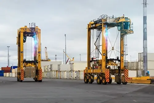
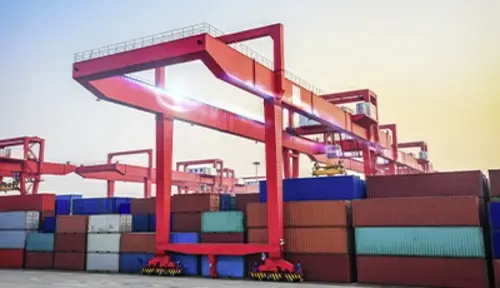
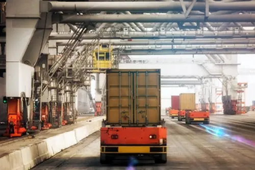
VAHLE Port Technology
Innovative solutions for the ports of tomorrow

Zero emission is the requirement for the port of the future. With the solutions for energy and data transmission from VAHLE, port operators are getting closer to this goal.

Discover solutions
VAHLE Amusement Rides Ferris Wheel
Intelligent solutions for the rides of the future

The amusement, leisure and adventure sectors are often at the cutting-edge of the industry. That's why many ride builders and manufactures rely on VAHLE to provide roller coaster and ride passengers with increasingly extraordinary experiences. 

Discover solutions
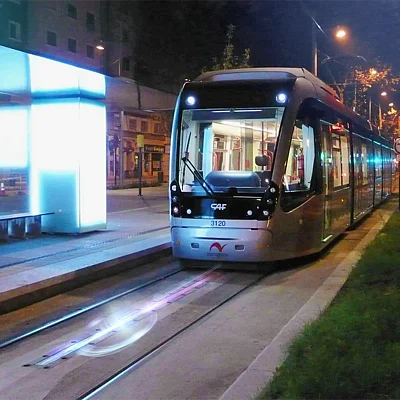
VAHLE People Mover Trams
Automated transport systems for the mobility of the future

Streetcars, sky trains or rolling sidewalks are the future of resource-saving mobility. Many manufacturers rely on components from VAHLE for the design.

Discover solutions
VAHLE General Industry
Innovative solutions for special mobile applications

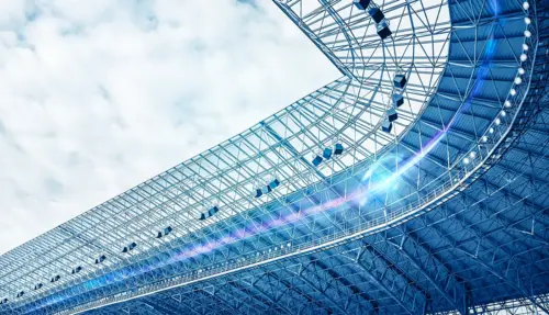
Stadium roofs, waste incineration plants, facade elevators: Mobile industrial applications are used in many areas. VAHLE offers various special solutions for reliable energy supply and data communication.

Discover solutions
产品
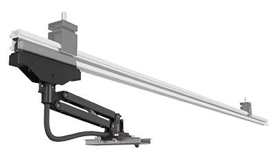
VAHLE data communication
Data communication: fast, flexible and secure

Advancing digitization requires the transmission of ever greater volumes of data. Our vCOM solutions ensure reliable data communication for the control of automated conveyor systems at all times.

Solutions for data communication
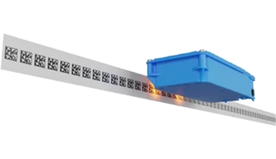
VAHLE positioning
Positioning: robust, flexible and precise

Modern manufacturing requires automated conveyor systems that can be positioned with extreme precision. The prerequisites for this are created by our robust vPOS solutions, which are available with both magnetic and optical processes.

Solutions for positioning
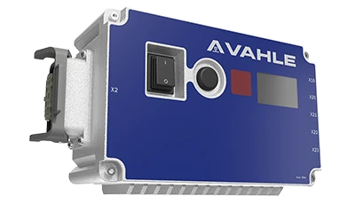
VAHLE control
Control: mobile, scalable and efficient

Automation is shaping modern production processes more than ever. Numerous mobile conveyor units must be reliably controlled. With our versatile vDRIVE solutions, this can be achieved flexibly and with optimized performance.

Solutions for control systems
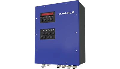
VAHLE system solution
System solutions: Everything from a single source

With our holistic system solutions, we offer a perfectly coordinated product combination of power transmission, data communication, positioning and control for a wide range of applications.

Discover system solutions
服务
VAHLE Services
法勒提供全方位的服务与支持,涵盖安装调试、维护维修、备件管理及培训等领域。如有需要,我们亦可作为总承包商为您的项目提供服务。
公司
VAHLE Unternehmen
我们是谁?我们从何而来?我们的未来将通向何方?在公司页面中,您可以全面了解法勒集团的公司历程、最新动态及成功客户案例。当然,这里也提供了我们的地理位置和联系方式。
职业生涯
VAHLE Karriere
了解家族企业的幕后故事。在我们的职业板块,您可以了解法勒集团的日常工作生活与职位详情、培训与进修机会,以及当前的空缺职位。别犹豫:我们一直在寻找充满热情的新同事!

From the wafer to the finished chip.

How is a semiconductor chip made?

Semiconductor chips form the foundation of modern technologies. They are found in smartphones, electric cars, medical devices and industrial equipment. Their manufacture combines high-precision production processes, complex automation and a precisely coordinated flow of materials.

But how does a piece of high-purity silicon become a functional semiconductor chip? The journey from wafer to finished chip involves numerous coordinated process steps – from the fabrication of the electronic structures in the wafer fab to die separation and subsequent IC packaging.

How is a semiconductor chip manufactured?

A semiconductor chip is produced in several successive manufacturing stages. In the wafer fab, the chip’s electronic structures are built up on a silicon wafer through repeated processes such as layer deposition, lithography, etching and doping. The wafer is then tested and separated into individual ‘dies’. 

In IC packaging, these dies are electrically connected, mechanically protected and prepared for their subsequent use.


Put simply, the process can be illustrated as follows:

Silicon → Wafer → Wafer fab → finished chip structures → Die separation → Die → IC packaging → finished chip

From the wafer fab to the finished chip

The actual electronic structures are manufactured in the wafer fab, known as the ‘front-end’ of semiconductor production. There, the wafers are processed in numerous steps under extremely controlled conditions.

The wafer as the starting point

Production begins with high-purity silicon. Thin slices are cut from a silicon crystal, ground and polished with high precision. These wafers form the basis for further chip manufacturing.

Many identical chip structures are fabricated simultaneously on a single wafer. Once fabrication is complete, these structures are separated from one another and processed further as individual dies. The number of dies produced on a wafer depends, amongst other things, on the wafer size and the area of the respective chip structure.


What happens in the wafer fab?

Manufacturing in the wafer fab consists of numerous sequential and repetitive process steps. These include, amongst others, the deposition of material layers, photolithography, etching and doping.

These processes are used to build up the various structures and layers of a chip step by step. In the process, the individual layers must be aligned with the utmost precision.

Lithography and etching

In lithography, the circuit pattern is transferred onto a photosensitive layer on the wafer using light. During the subsequent etching process, material is selectively removed from the designated areas. This creates the fine structures from which the chip’s electronic components are later built.

Layer deposition and doping

In layer deposition, wafer-thin layers of conductive, insulating or semiconducting materials are deposited onto the wafer. Through doping, foreign atoms are selectively introduced into the semiconductor material in order to alter its electrical properties. This allows, amongst other things, the creation of the different electrical regions required for transistors.

Metallisation

Metallisation is the process by which the electrical connections within the chip are formed. This involves creating several wiring layers that connect individual transistors and functional blocks to one another. In this way, the complex network of conductors that electrically links the various areas of the chip is gradually formed.

Layer by layer:

A recurring process

These steps are not carried out just once. Layer deposition, lithography, etching, doping and other process steps are repeated over and over again to build up the chip’s various layers and structures.

This is how, layer by layer, the complex architecture of a modern semiconductor is created. In the process, the individual structures must be aligned with one another with the utmost precision during each cycle. It is only through the interplay and repeated execution of these processes that the silicon wafer is transformed into a highly complex chip structure containing a large number of transistors and electrical connections.


From the wafer to the individual die

Once production is complete, the wafer contains many individual chip structures. Before these are processed further, the finished structures are inspected and then separated from one another.

During the separation process, also known as dicing, the wafer is divided into individual chip structures along the designated cutting lines. These individual, as yet unpackaged chip structures are referred to as dies.

This marks the completion of the manufacture of the electronic structures. 

The next step is packaging.

From die to finished chip

What happens during IC packaging?

Following wafer fabrication and die separation, the individual die undergoes IC packaging. IC packaging stands for ‘Integrated Circuit Packaging’ and refers to the processes by which the chip is electrically connected, mechanically protected and prepared for its subsequent use.

Why does a chip need packaging?

An unpackaged die is delicate and cannot easily be integrated into an electronic system. Packaging therefore fulfils several important functions.

Among other things, it provides:

  • electrical connection points for linking to the printed circuit board or other components
  • mechanical protection of the sensitive die
  • thermal management to dissipate heat generated
  • reliable integration of the chip into the relevant electronic system


Depending on the application, different packaging technologies are used. These include, for example, bond wires, flip-chip connections, microbumps and other interconnect technologies.

What are the functions of packaging?

IC packaging connects the finished die to the outside world. To achieve this, electrical connections are made to the chip and it is integrated into a suitable housing or package structure.

At the same time, the packaging protects the die from mechanical stress and external influences. Heat dissipation also plays an important role, as modern chips can generate considerable amounts of heat during operation.


The result is a component that can be integrated into an electronic system and used reliably within it.

  • Electrical connection: Contact via bond wires, microbumps or interconnects
  • Mechanical protection: Protection against environmental influences and stresses
  • Thermal management: Dissipation of generated heat
  • Integration: Higher packing density and improved performance

Why are cleanrooms and material flow so important in semiconductor production?

The manufacture of semiconductors places high demands not only on the manufacturing processes themselves. The environment in which these processes take place and the transport of materials are also crucial.

During their manufacture, wafers must pass through numerous pieces of equipment and process steps. At the same time, their quality must not be compromised by particles, vibrations or other external influences.

How clean is a cleanroom in semiconductor production?

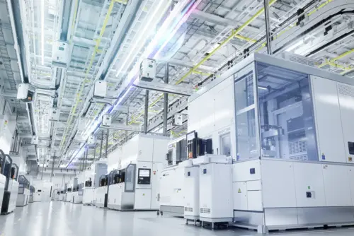
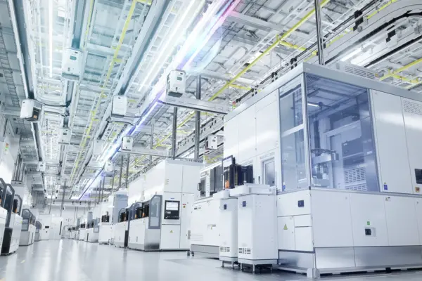
Cleanrooms in classes ISO 1–5 filter even the tiniest particles out of the air. Even the smallest contaminants can destroy structures and render entire process steps unusable.

How does the material flow work in a wafer fab?

During production, systems transport the wafers hundreds of times between machines. This transport is:

  • contact-free
  • with minimal vibration
  • fully automated
  • under cleanroom conditions

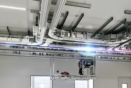
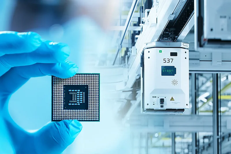
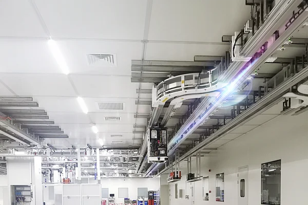
Overhead transport systems (OHT) perform this task and form the backbone of in-house logistics within the cleanroom.

What role does the flow of materials play in production?

A stable flow of materials helps to ensure:

  • short and predictable lead times
  • high plant availability
  • consistent production conditions
  • a high yield
  • reliable production processes


The more complex the manufacturing processes become, the more important it is to have precisely coordinated automation of material handling

How do Fab and Packaging work together?

Semiconductor production can only take place when both areas work together.

  • The circuits are manufactured in the fab
  • In the packaging department, these are turned into a usable component

Together, they determine:

  • Speed
  • Energy efficiency
  • Reliability
  • Latency
  • Service life
  • Thermal stability

As modern chips become increasingly complex, these two areas are becoming ever more intertwined.

What role does the flow of materials between the fab and packaging play?

The material flow links all the process steps in semiconductor production. 

Wafers and dies pass through testing processes, transitions between production stages and transport between production lines. 

Any disruption has a direct impact on the entire value chain.

A stable, continuous material flow is crucial to production reliability, efficiency and the quality of the end product.

Why is semiconductor production considered to be particularly challenging?

The manufacture of semiconductors is one of the most technically demanding industrial production processes. Numerous process steps must be precisely coordinated with one another. At the same time, there are high standards regarding cleanliness, precision, automation and availability.

What are the key requirements in semiconductor manufacturing?

Among the most important requirements in the production of semiconductors are

  • cleanrooms of the highest classes
  • Nanometre precision
  • 24/7 operation
  • a high degree of automation
  • complex process dependencies

Why are defects in semiconductor production so costly?

Even minor disruptions can have major consequences:

  • Production stoppages hold up entire production lines
  • Even the tiniest contaminants can ruin entire batches
  • Thermal issues reduce the service life of chips

How global is the organisation of semiconductor production?

Value creation is spread across the globe:

  • Wafer production in one country
  • Packaging in another
  • Final assembly at a third location

This global structure further increases the complexity.

How will semiconductor production develop in the future?

The semiconductor industry is constantly evolving. Increasing demands for computing power, energy efficiency and integration density are driving the development of new manufacturing and packaging technologies.

Key developments include:

3D integration and advanced packaging

In 3D integration, multiple chip structures or dies are connected vertically or in a particularly compact configuration. This makes it possible to shorten signal paths, increase data transfer rates and improve the energy efficiency of the overall system. In addition, advanced packaging enables the highly integrated combination of different chips or chiplets within a single package. This technology allows different functions – such as computing power, memory and communication units – to be combined in a particularly high-performance and space-saving manner.


Chiplet architectures

In chiplet architectures, a complex system is not necessarily implemented as a single large chip. Instead, several smaller, functionally specialised dies can be combined with one another.

This enables a flexible combination of different functions and can offer advantages in terms of development, manufacturing and system integration.


Co-packaging of electronics and photonics

Electronic and optical components can increasingly be integrated together within a single package. Particularly in applications with high demands on data transmission and bandwidth, this close integration can open up new possibilities for high-performance and energy-efficient systems.


AI-supported process optimisation

The increasing digitalisation of manufacturing enables the analysis of large volumes of production and process data. Artificial intelligence and data-driven methods can help to monitor processes, detect deviations at an early stage and further optimise production workflows.


Greater automation and intelligent material flows

As manufacturing becomes increasingly complex, so too do the demands placed on automation. Wafers and dies must be moved reliably and at the right time between an ever-increasing number of process steps and pieces of equipment.

Consequently, the importance of intelligent and highly available material flow systems is also growing.

Why are OHT systems and power transmission becoming increasingly important?

The more complex semiconductor production becomes, the more important a stable and automated material flow becomes. OHT systems handle the transport of wafers and materials within the production environment.

To ensure these systems can operate continuously, they require a reliable power supply. In cleanrooms in particular, there are specific requirements regarding availability, maintenance requirements and environmental conditions.

Reliable power transmission systems support this:

  • continuous transport
  • high system availability
  • automated production processes
  • low particle load
  • reliable operating conditions


The power supply thus becomes a key component of the infrastructure that enables the automated flow of materials in semiconductor production.

Semiconductor manufacturing: Where precision and material flow come together

The manufacture of a semiconductor chip involves the interplay of many high-precision processes. Complex electronic structures are created from a silicon wafer through numerous repetitive manufacturing steps. After dicing, the individual dies are connected, protected and prepared for their respective applications during the packaging process.

To ensure that these processes interlock reliably, a stable and automated material flow is required in addition to state-of-the-art manufacturing technology.

Material flow, automation and power supply are therefore key components of high-performance semiconductor production.

How VAHLE supports semiconductor production

VAHLE supports semiconductor manufacturers worldwide with solutions for safe and reliable power transmission in highly automated production and cleanroom environments.

VAHLE’s systems are designed to reliably supply power to overhead transfer systems (OHT) and other material-handling systems. In this way, they help ensure that automated transport systems can operate continuously under the demanding conditions of semiconductor production.


The focus is on:

  • reliable power transmission
  • high availability
  • low-maintenance systems
  • suitability for highly automated production environments
  • Requirements for cleanliness and precision

Making semiconductor production more efficient now

Would you like to future-proof your semiconductor production and optimise your material flow?

VAHLE recommends investing in reliable power transmission systems at an early stage.
 

Get personalised advice

Further links

Our solutions

Contactless power transfer with the CPS140

Find out more
Application

OHT systems for high-precision production environments

Find out more
Market

Where every particle counts – cleanrooms

Find out more

您当地的联系人

您所在的地区:
请输入正确的地址

您的联系方式