- Customer Hub
- Trade show
- Downloads
- Contact
-
Choose desired country organisation:
-
Choose your language:


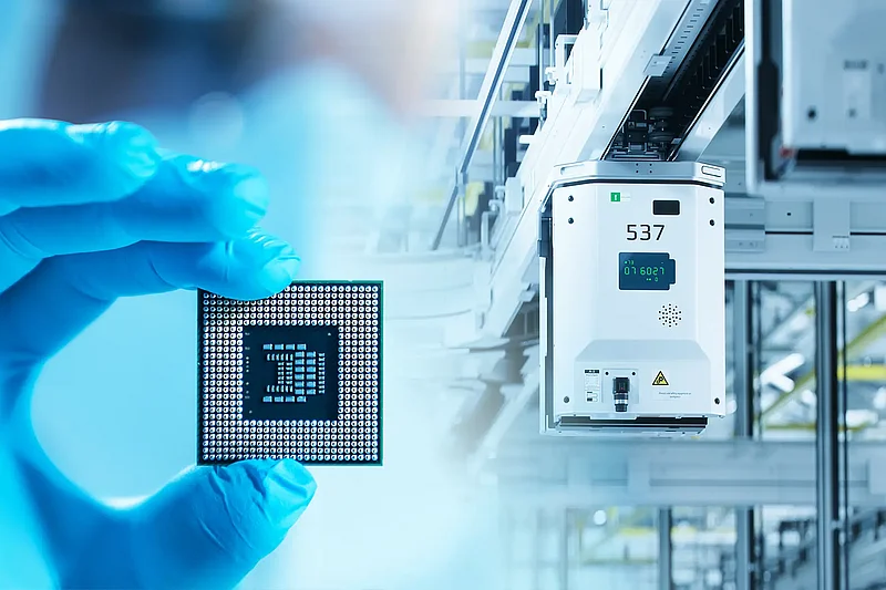
Semiconductor chips form the foundation of modern technologies. They are found in smartphones, electric cars, medical devices, and industrial equipment. Their production combines high-precision manufacturing processes, complex automation, and a precisely coordinated flow of materials.
But how does a piece of high-purity silicon become a functional semiconductor chip? The journey from wafer to finished chip involves numerous coordinated process steps—from the fabrication of electronic structures in the wafer fab to die separation and subsequent IC packaging.
A semiconductor chip is produced in several successive manufacturing stages. In the wafer fab, the chip’s electronic structures are built up on a silicon wafer through repeated processes such as layer deposition, lithography, etching, and doping. The wafer is then tested and separated into individual dies.
In IC packaging, these dies are electrically connected, mechanically protected, and prepared for their future use.
Silicon → Wafer → Wafer fab → Finished chip structures → Separation → Die → IC packaging → Finished chip

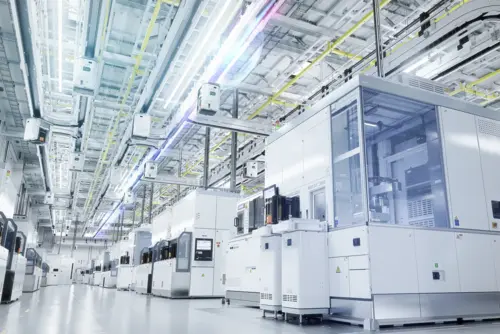
The actual electronic structures are manufactured in the wafer fab, known as the front end of semiconductor production. There, the wafers are processed in numerous steps under extremely controlled conditions.
Production begins with high-purity silicon. Thin slices are cut from a silicon crystal, ground, and polished with high precision. These wafers form the basis for further chip manufacturing.
Many identical chip structures are fabricated simultaneously on a single wafer. Once fabrication is complete, these structures are separated from one another and processed further as individual dies. The number of dies produced on a wafer depends, among other factors, on the wafer size and the area of the respective chip structure.
Manufacturing in the wafer fab consists of numerous sequential and repetitive process steps. These include, among other things, the deposition of material layers, photolithography, etching, and doping.
These processes are used to build up the various structures and layers of a chip step by step. In the process, the individual layers must be aligned with the highest precision.
These steps are not performed just once. Layer deposition, lithography, etching, doping, and other process steps are repeated over and over again to build up the chip’s various layers and structures.
This is how the complex architecture of a modern semiconductor is created, layer by layer. In the process, the individual structures must be aligned with each other with the utmost precision during each cycle. It is only through the interplay and repeated execution of these processes that the silicon wafer is transformed into a highly complex chip structure containing a large number of transistors and electrical connections.
Once manufacturing is complete, the wafer contains many individual chip structures. Before these are processed further, the finished structures are inspected and then separated from one another.
During the separation process, also known as dicing, the wafer is divided into individual chip structures along the designated cutting lines. These individual, unpackaged chip structures are referred to as dies.
This completes the fabrication of the electronic structures.
The next step is packaging.

After wafer fabrication and die separation, the individual die undergoes IC packaging. IC packaging stands for “Integrated Circuit Packaging” and refers to the processes used to establish electrical connections to the chip, protect it mechanically, and prepare it for its future use.
An unpackaged die is delicate and cannot be easily integrated into an electronic system. Packaging therefore serves several important purposes.
Among other things, it provides:
Depending on the application, different packaging technologies are used. These include, for example, bond wires, flip-chip connections, microbumps, and other interconnect technologies.
IC packaging connects the finished die to the outside world. To do this, electrical connections are made to the chip, and it is integrated into a suitable housing or package structure.
At the same time, the packaging protects the die from mechanical stress and external influences. Heat dissipation also plays an important role, as modern chips can generate significant amounts of heat during operation.
The result is a component that can be integrated into an electronic system and used reliably there.
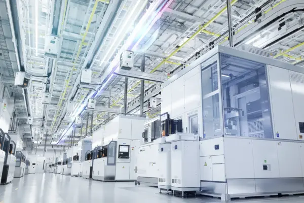
Semiconductor manufacturing places high demands not only on the manufacturing processes themselves, but also on the environment in which these processes take place and the transportation of materials.
During production, wafers must pass through numerous pieces of equipment and process steps. At the same time, their quality must not be compromised by particles, vibrations, or other external influences.
Semiconductor production is only possible when both areas work together.
Together, they determine:
As modern chips become increasingly complex, these two areas are increasingly converging.

The material flow connects all process steps in semiconductor production.
Wafers and dies undergo testing, move between production stages, and are transported between equipment.
Any disruption has a direct impact on the entire value chain.
A stable, continuous material flow is crucial for production reliability, efficiency, and the quality of the final product.
Semiconductor manufacturing is one of the most technically demanding industrial production processes. Numerous process steps must be precisely coordinated with one another. At the same time, there are high requirements for cleanliness, precision, automation, and availability.
The semiconductor industry is constantly evolving. Increasing demands for computing power, energy efficiency, and integration density are driving the development of new manufacturing and packaging technologies.
Key developments include:
3D Integration and Advanced Packaging
In 3D integration, multiple chip structures or dies are connected vertically or in a particularly compact configuration. This shortens signal paths, increases data transfer rates, and improves the energy efficiency of the overall system. In addition, advanced packaging enables the highly integrated combination of different chips or chiplets within a single package. This technology allows for the combination of different functions—such as computing power, memory, and communication units—in a highly efficient and space-saving manner.
Chiplet Architectures
In chiplet architectures, a complex system is not necessarily implemented as a single large chip. Instead, several smaller, functionally specialized dies can be combined.
This enables a flexible combination of different functions and can offer advantages in development, manufacturing, and system integration.
Co-Packaging of Electronics and Photonics
Electronic and optical components can increasingly be integrated together within a single package. Especially in applications with high demands on data transmission and bandwidth, this close integration can create new opportunities for high-performance and energy-efficient systems.
AI-Driven Process Optimization
The increasing digitization of manufacturing enables the analysis of large volumes of production and process data. Artificial intelligence and data-driven methods can help monitor processes, detect deviations early on, and further optimize production workflows.
Greater Automation and Intelligent Material Flows
As manufacturing becomes more complex, the demands on automation also increase. Wafers and dies must be moved reliably and at the right time between an ever-growing number of process steps and pieces of equipment.
Consequently, the importance of intelligent and highly available material flow systems is also growing.
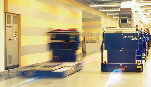
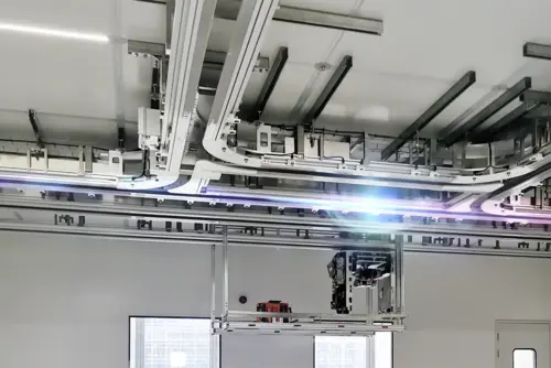
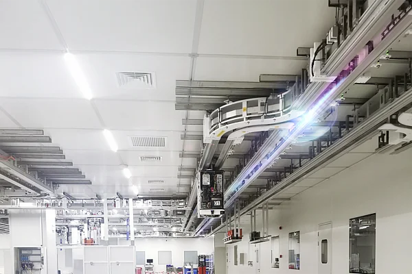
The more complex semiconductor production becomes, the more important a stable and automated material flow becomes. OHT systems handle the transport of wafers and materials within the production environment.
To ensure these systems can operate continuously, they require a reliable power supply. Cleanrooms, in particular, have specific requirements regarding availability, maintenance, and environmental conditions.
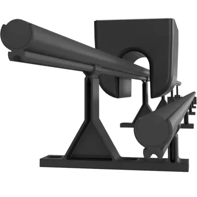
Reliable power transmission systems support this:
reliable operating conditions
The power supply thus becomes a key component of the infrastructure that enables automated material flow in semiconductor production.
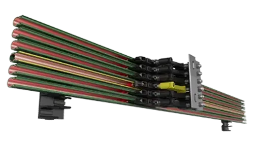
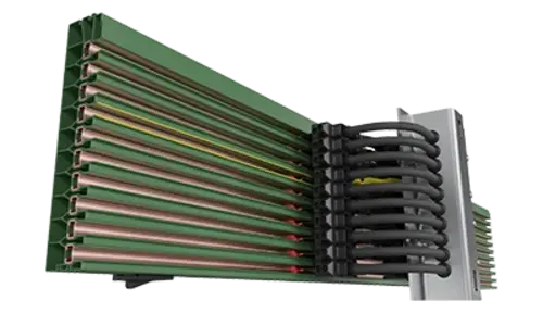
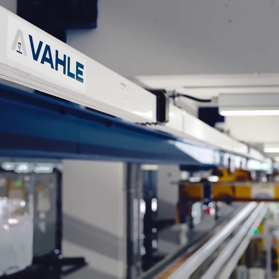
VAHLE supports semiconductor manufacturers worldwide with solutions for safe and reliable power transmission in highly automated production and cleanroom environments.
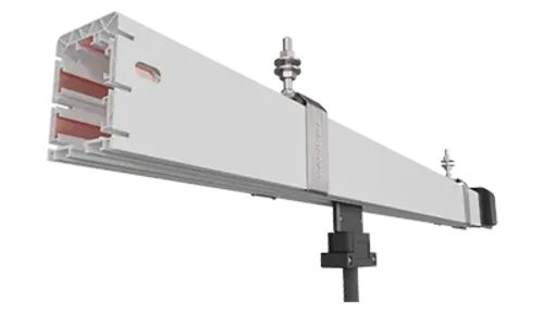
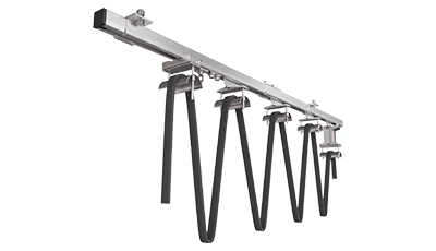
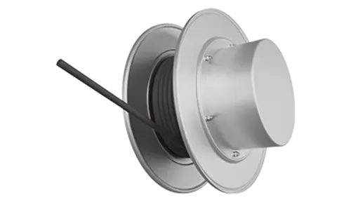
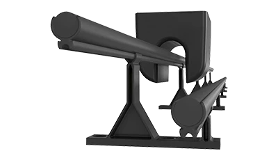
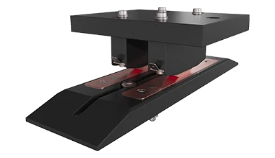
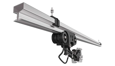
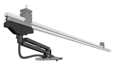
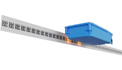
VAHLE’s systems are designed to reliably supply power to overhead transfer (OHT) and other material handling systems. In this way, they help ensure that automated transport systems can operate continuously under the demanding conditions of semiconductor production.
{{ selectedCountry.title }}